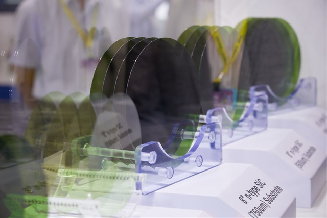
Infineon announced that it has succeeded in developing the world's first 300mm GaN wafer technology for power electronics. This allows for the improvement of efficiency performance, smaller size, lighter weight, and lower overall cost for the chips.

According to Infineon, the breakthrough will help the company to significantly advance the market for GaN-based power semiconductors. Chip production on 300-millimetre wafers is technologically more advanced and much more efficient than on 200-millimetre wafers, as the larger wafer diameter enables 2.3 times the number of chips per wafer to be produced. Infineon writes that the new production process “enables efficiency performance, smaller size, lighter weight, and lower overall cost. Furthermore, 300 mm manufacturing ensures superior customer supply stability through scalability.”
Infineon also estimates that being able to use its existing 300 mm silicon manufacturing equipment, “since gallium nitride and silicon are very similar in manufacturing processes. Infineon’s existing high-volume silicon 300 mm production lines are ideal to pilot reliable GaN technology, allowing accelerated implementation and efficient use of capital.”
“This remarkable success is the result of our innovative strength and the dedicated work of our global team to demonstrate our position as the innovation leader in GaN and power systems,” said Jochen Hanebeck, CEO of Infineon Technologies AG. “The technological breakthrough will be an industry game-changer and enable us to unlock the full potential of gallium nitride. Nearly one year after the acquisition of GaN Systems, we are demonstrating again that we are determined to be a leader in the fast-growing GaN market. As a leader in power systems, Infineon is mastering all three relevant materials: silicon, silicon carbide and gallium nitride.”
Infineon recently also opened a new semiconductor production facility in Malaysia, which focuses on silicon carbide converters. The company has also been researching a semiconductor project with GaN since May 2025.


최신 산업 동향을 받아보려면 구독하세요.저희 뉴스레터는 전문가가 제공드리는 가치있는 시장 정보입니다.
The US has initiated a Section 301 investigation into China's mature semiconductor processes and third-generation silicon carbide (SiC) semiconductors. Supply chain operators state that the increa

In 2025, we expect 9.5% growth in the global semiconductor market, driven by robust demand for data centre services, including AI. However, growth in other, more mature segments is expected to be stag

Taiwanese chip manufacturer TSMC has announced a $100 billion investment in the United States, aiming to build five additional semiconductor facilities.The plan was revealed by TSMC CEO C.C. Wei along

Prices of mature process memory, long hit by oversupply due to fast capacity expansion at Chinese makers, are expected to rebound, thanks to the Chinese government's consumption stimulus programs.
With the ongoing development of new-generation processors, the introduction of PCIe Gen5 specifications into high-end PC applications is set to commence in 2025. According to Micron Technology, Gen4 p
The global market is watching how TSMC, pressured by the US, might assist Intel's foundry operations, while Samsung Electronics and Rapidus, also facing challenges, may similarly require TSMC'


