
Samsung Electronics is reportedly preparing to introduce its first High-NA EUV (extreme ultraviolet lithography) equipment in early 2025, signaling a major advancement for the South Korean tech leader in the realm of advanced semiconductor manufacturing. This cutting-edge technology, exclusively provided by Dutch firm ASML, is essential for processes below the 2nm threshold. Industry watchers in South Korea anticipate that Samsung will accelerate its development efforts toward commercializing 1nm chips.
According to ET News, Samsung's first High-NA EUV tool, the EXE:5000 model from ASML, is expected to arrive in early 2025. Given the complexity of semiconductor equipment installation, which typically involves lengthy testing phases, the EXE:5000 is projected to be operational by the second quarter of 2025.
High-NA EUV technology surpasses existing EUV systems by enabling the creation of finer circuit designs, making it suitable for semiconductors like CPUs and GPUs that operate below 5nm. While standard EUV is effective for 5nm processes and below, High-NA EUV can achieve circuit sizes under 2nm, thereby enhancing performance and reducing the number of exposure cycles, thus lowering production costs. Recent research from the Belgian center Imec, in collaboration with ASML, demonstrated that a single High-NA EUV exposure can produce complete logic and memory circuits.
This development marks Samsung's first foray into High-NA EUV technology. Previously, the company has collaborated with Imec on circuit processing research. With its own equipment, Samsung aims to accelerate its development of advanced nodes, setting a target to commercialize a 1.4nm process by 2027, which could pave the way toward 1nm production.
On a global scale, the competition among semiconductor giants like TSMC, Intel, and Samsung is heating up as they race to secure High-NA EUV tools for processes below 2nm. Intel was the first to obtain its unit in December 2023, followed by TSMC in the third quarter of 2024. Although Samsung's order comes later, achieving stable production may be the key factor in determining industry leadership.
Samsung plans to use the High-NA EUV equipment expected in early 2025 for research purposes, with plans to introduce dedicated mass-production units soon after. During a meeting with ASML in the third quarter of 2024, Samsung indicated it would reconsider the number of High-NA EUV units it plans to acquire, potentially reducing its initial order by two units. The company originally aimed to introduce the EXE:5000 by the fourth quarter of 2024, with subsequent models—EXE:5200, EXE:5400, and EXE:5600—set to be rolled out over the next decade.


최신 산업 동향을 받아보려면 구독하세요.저희 뉴스레터는 전문가가 제공드리는 가치있는 시장 정보입니다.
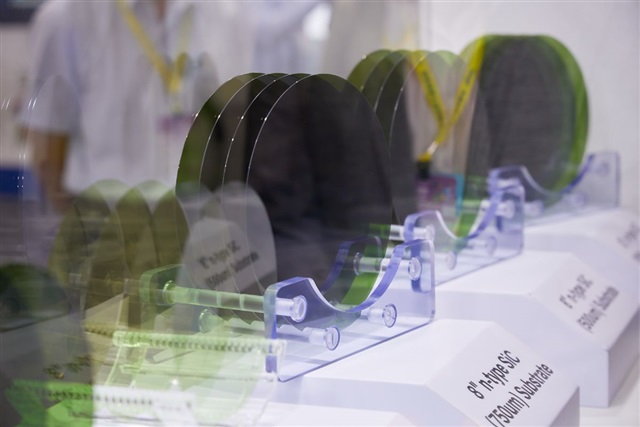
The US has initiated a Section 301 investigation into China's mature semiconductor processes and third-generation silicon carbide (SiC) semiconductors. Supply chain operators state that the increa
In 2025, we expect 9.5% growth in the global semiconductor market, driven by robust demand for data centre services, including AI. However, growth in other, more mature segments is expected to be stag

Taiwanese chip manufacturer TSMC has announced a $100 billion investment in the United States, aiming to build five additional semiconductor facilities.The plan was revealed by TSMC CEO C.C. Wei along

Prices of mature process memory, long hit by oversupply due to fast capacity expansion at Chinese makers, are expected to rebound, thanks to the Chinese government's consumption stimulus programs.
With the ongoing development of new-generation processors, the introduction of PCIe Gen5 specifications into high-end PC applications is set to commence in 2025. According to Micron Technology, Gen4 p
The global market is watching how TSMC, pressured by the US, might assist Intel's foundry operations, while Samsung Electronics and Rapidus, also facing challenges, may similarly require TSMC'


